Laser lithography is taking semi-conductor production by storm – new nano-material produced
In the past integrated circuits have been manufactured using so called photolithography – lasers have simplified the process and opened up new opportunities
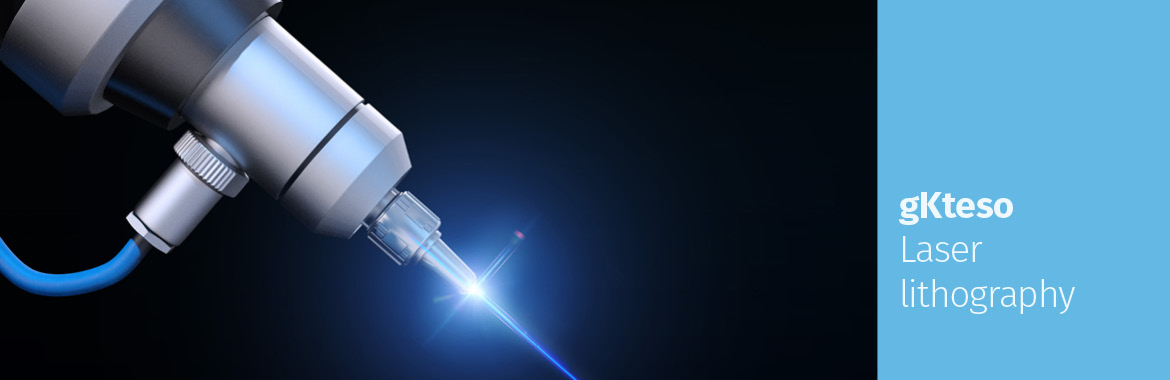
In photolithography the image of a photomask is projected onto a light-sensitive coating by the exposure process. Depending on the process used, the exposed or unexposed areas of the photoresist are then dissolved using chemicals. This results in a lithographic mask which can be used as the basis for integrated circuits. Laser lithography uses the energy in the laser beam to harden the required areas in the photoresist. Chip production has reached a whole new level as a result of the development of highly efficient laser lithography systems.
Pulsed CO2 laser for laser lithography
New technical developments in the CO2 laser have made it possible to increase the peak pulse rating to several megawatts. This makes it suitable for use in laser lithography. And development work is continuing – researchers have created a new material through laser lithography and subsequent pyrolysis. This is a so-called meta-material which copies Mother Nature. Bone structures or wood combine high strength with relatively low weight. Meta-materials are planned and manufactured with similar structures just a few micrometres in size. This means that they can have optical or mechanical properties which unstructured solids cannot match. For the new nano-material, the required structure, just micrometres in size, is transferred to photoresist using 3-D laser lithography. To make it even smaller, the researchers shrink the structure using pyrolysis and glazed the lattice whose struts have a diameter of 0.2 micrometres.
The micro-structured materials manufactured in this way are used for insulation purposes, as shock absorbers or as filters in the chemical industry. But the optical properties of the micro-materials are also of interest for telecommunications. Micro-structured glassy carbon combines the ceramic properties of glass with those of graphite and can be used as a material in electrodes on batteries or also in electrolysis systems.
For further information about gKteso laser beam systems, send a mail to info@gkteso.de.

 Download Datasheets