Wafer scribing with a laser makes wafer sawing superfluous
Wafers can be scribed with a laser at a rate of 300 to 700 millimetres per second – faster than any saw.
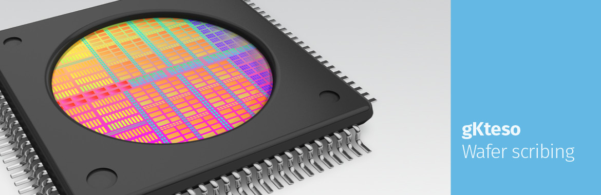
Wafers are very thin circular or square discs used as panels in photovoltaics, microelectronics and micro-system engineering. Often chips are particularly manufactured en masse. These chips must be supplied individually before undergoing further processing. In the case of silicium wafers or wafers to be used as semi-conductors, tiny partition frames are inserted between the individual chips. This narrow area is destroyed by wafer scribing. To continue to use the individual chips, they are affixed to an adhesive foil, generally so-called blue foil, before the wafer scribing process. The foil must have certain properties to make it suitable for this process, for example it must be manufactured in a clean room.
Cutting by wafer scribing with a laser, diamond or saw?
The conventional methods for cutting the wafers include wafer scribing with a diamond point. This is done by applying slight pressure over the scribing area so as to produce minimal recesses. This method is used to produce desired defects and stresses in the crystal structure of the wafers which then break when the scribed point is stressed slightly. However, the thicker the wafer becomes, the more difficult wafer scribing is using a diamond. Furthermore, the scribing and subsequent breaking of the wafers result in jagged edges which make it more difficult to grip the chips during further use. Diamond-tipped cutting discs are guided along the cutting lines for sawing the wafers. Since silicium dust is produced by this process, the wafers then have to be rinsed in fluid.
Wafer scribing with a laser avoids these problems. Even thick wafers can be cut easily and with precise edges. When the blue foil is then expanded, the chips are easy to grip and can be processed cleanly. In contrast to mechanical scribing, the material in the scribing area undergoes limited localised melting in the wafer scribing process using a laser. This crystallises it to form poly-crystalline silicium. This forms the desired stresses in the material which make it easy to break.
Wafer scribing using a laser is cost-effective, requires significantly less time than conventional methods and requires no etching or rinsing fluids. Let us persuade you – we will be delighted to advise you. Send a mail to info@gkteso.de.

 Download Datasheets