Laser annealing – deep activation of implants
Microelectronics, photovoltaics and microsystem technology are now completely dependent on wafers
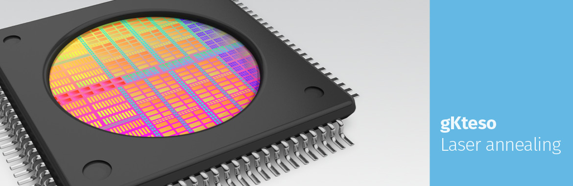
Wafers are discs around one millimetre thick. They are manufactured from semi-conductor blanks and are generally shaped using a laser. A wafer is used as a base plate for electronic components or photoelectric coatings. To prepare them for additional stages, the wafers are “doped”, which means that charged ions are accelerated in an electrical field and directed at the wafers. They are thus charged with ion implants so as to influence the electrical properties. Laser annealing is the process with which these ion implants can be activated. Laser annealing has plenty of benefits compared to conventional processes such as the furnace process. For example, laser annealing does not damage the protective foil on the front of the wafers because the process does not overheat the wafer or foil. Furthermore laser annealing ensures that the implants undergo uniform deep activation. The non-homogeneous temperature distribution in the furnace process results in the lower activation of the implants. Moreover, laser annealing is used to recrystallise amorphous surfaces on semi-conductors. This means that the processes particularly in demand in microelectronics to recrystallise semi-conductors which have previously been amorphised by ion implantation.
Flat displays for mobile devices are only possible using laser technology
It will soon be possible to use the process to apply polycrystalline silicium to glass for flat displays on foils as well. It will then be possible to manufacture unbreakable displays, for example a mobile device which can simply be rolled up and placed in your pocket but nevertheless is unbreakable. These developments have been made possible thanks to progress in laser technology which plays a major role in the crystallisation process for the displays in the form of laser annealing.
Are you interested in a laser beam system? Then write to us, will be delighted to advise you about what is possible for your application. Simply send a mail to info@gkteso.de.

 Download Datasheets